Final Exam
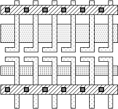
1. Lay out a buffer with a stage ratio 1:3 (3 parallel inverters driven by an inverter) on the following SOG. Remember that you can use a turned-off transistor to split the diffusion lines. (10%)
2. Design a scan cell and then synthesize a full scan chain for the following circuit CUT to CUT_S0. (10%)
module CUT(Clk, A, B, C, E);
input Clk, A, B, C;
output E;
dff FF1(.clk(Clk), .q(E), .d(F));
nand g1(F, A, B), g2(G, F, C);
nor g3(H, I, G);
dff FF2(.clk(Clk), .q(I), .d(H));
endmodule
3. Neglecting the jitters, skews, setup time and clock-to-Q times, let the propagation time of Finite State Machine Zi=Mi(Xi) be tQDi. What’s the propagation time of Z4=M4(M3(M1(X1), M2(X2)))? How is the IP rule used to reduce it? (10%)
4. Give at least 5 issues for IP reuse. (10%)
5. What are the four units in a typical processor? (10%)
6. Draw a digital IC design flow using tools from the CIC. (10%)
7. Explain bus contention and floating? How can we prevent them?(10%)
8. What structure do we usually use to implement a many-input NOR gate? What disadvantage does it have? How can we improve it? (10%)
9. Draw a CVSL schematic of a full adder, {Co, S}=A+B+Ci.(10%)
10. Draw the basic SRAM architecture introduced in this course. (10%)